
下载
PWM
Control
FET
Sync
FET
Input
Supply
L
O
I
L
C
O
Load
Driver
Driver
C
I
Switch
Node
Application Report
SLPA005 – June 2009
Reducing Ringing Through PCB Layout Techniques
David Jauregui ...................................................................................................... PMP - Power Stage
ABSTRACT
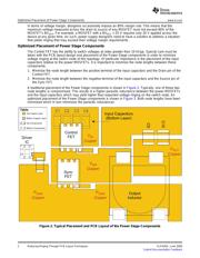
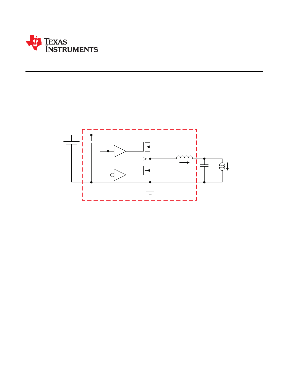
Designers must consider several topics when designing a printed-circuit board (PCB)
layout for a dc-to-dc converter. In particular, the layout of the Power Stage components
within a nonisolated synchronous buck converter requires special attention in order to
optimize the overall performance of the switching function. The Power Stage in this
application report is defined to include the input capacitors, power MOSFETs, driver IC,
and output inductor (see Figure 1 ).
Figure 1. Definition of Power Stage Components
This document discusses the topic of voltage ringing commonly found to be
superimposed on the rising edge of the switch node (V
SW
) waveform. It also describes
how to optimize the PCB layout design to minimize the magnitude of the ringing.
Background
The two major industry concerns toward the ringing commonly found to be superimposed on the switch
node waveform are:
1. Voltage Margin
• This is a percentage ratio which takes the magnitude of the first peak within the ringing waveform
and compares it to the breakdown voltage of the power MOSFET (BV
DSS
).
2. EMI/EMC
• This the amount of conducted or radiated noise produced by the ringing waveform.
This application report only addresses the topic of voltage margin and does not focus on the topic of
EMI/EMC. The topic of EMI/EMC can be somewhat subjective and greatly depends on the overall
system/chassis design. However, the enhancements outlined in this document can improve the overall
EMI/EMC performance of the system.
SLPA005 – June 2009 Reducing Ringing Through PCB Layout Techniques 1
Submit Documentation Feedback