
下载
© Semiconductor Components Industries, LLC, 2006
June, 2006 − Rev. 0
1 Publication Order Number:
AND8269/D
AND8269/D
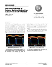
Layout Guidelines to
Reduce Switch−Node Jitter
in the CS51411/NCV51411
Prepared by: Jim Hill
ON Semiconductor
Introduction
The CS5141x product family has shown some sensitivity
to noise which shows up as jitter on the Switch Node pin
(VSW). The CS51411 family uses V
2
control to achieve
superior line and load. This control method enhances the
load transient response, but under certain conditions can
lead to jitter if proper care is not taken. V
2
performs similarly
to current mode control, but that the gain is much higher. The
gain is set up by the output ripple voltage plus the internal
ramp. As you decrease the output voltage, you also decrease
ripple voltage which, in turn, increases gain. With a high
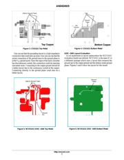
gain, the PCB layout becomes very critical. This report
shows how minor changes in layout can greatly improve
VSW jitter on the CS51411 family of buck converters.
Problem
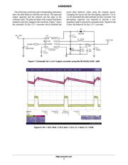
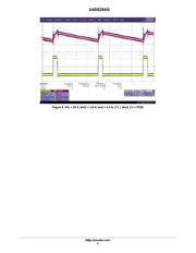
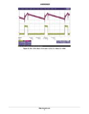
Figures 1 and 2 show examples of this jitter phenomenon.
The upper waveform (CH1) is the output voltage and the
lower waveform (CH2) is the voltage at VSW.
Figure 1. 18 VAC (24 VDC) to 1.8 V/1.4 A
Figure 2. 18 VAC (24 VDC) to 3.3 V/1.3 A
Notice that the jitter at the lower output voltage of 1.8 V
is much worse than that at 3.3 V which supports the claim in
the introduction. The customer was using the
ON Semiconductor evaluation board with their own
components when they noted this behavior.
APPLICATION NOTE
http://onsemi.com