
下载
© Semiconductor Components Industries, LLC, 2016
July, 2016 - Rev. 2
1 Publication Order Number:
AND9311/D
AND9311/D
Power-up Time
Acceleration
Overview
ON Semiconductor RF chip have typical start−up times
from sleep to oscillator and references running are in the
order of 3 ms (this value depends on the specific crystal
used). This time can vary with temperature and be in rare
cases over 10 ms. The start−up time is not specified and not
controlled. For synchronous applications this is not
desirable. Therefore we are presenting two easy ways to
reduce and control the start−up time to a constant value.
This document applies to the devices AX5051, AX5151,
AX5031, AX5131 and AX50424.
Power−up Acceleration
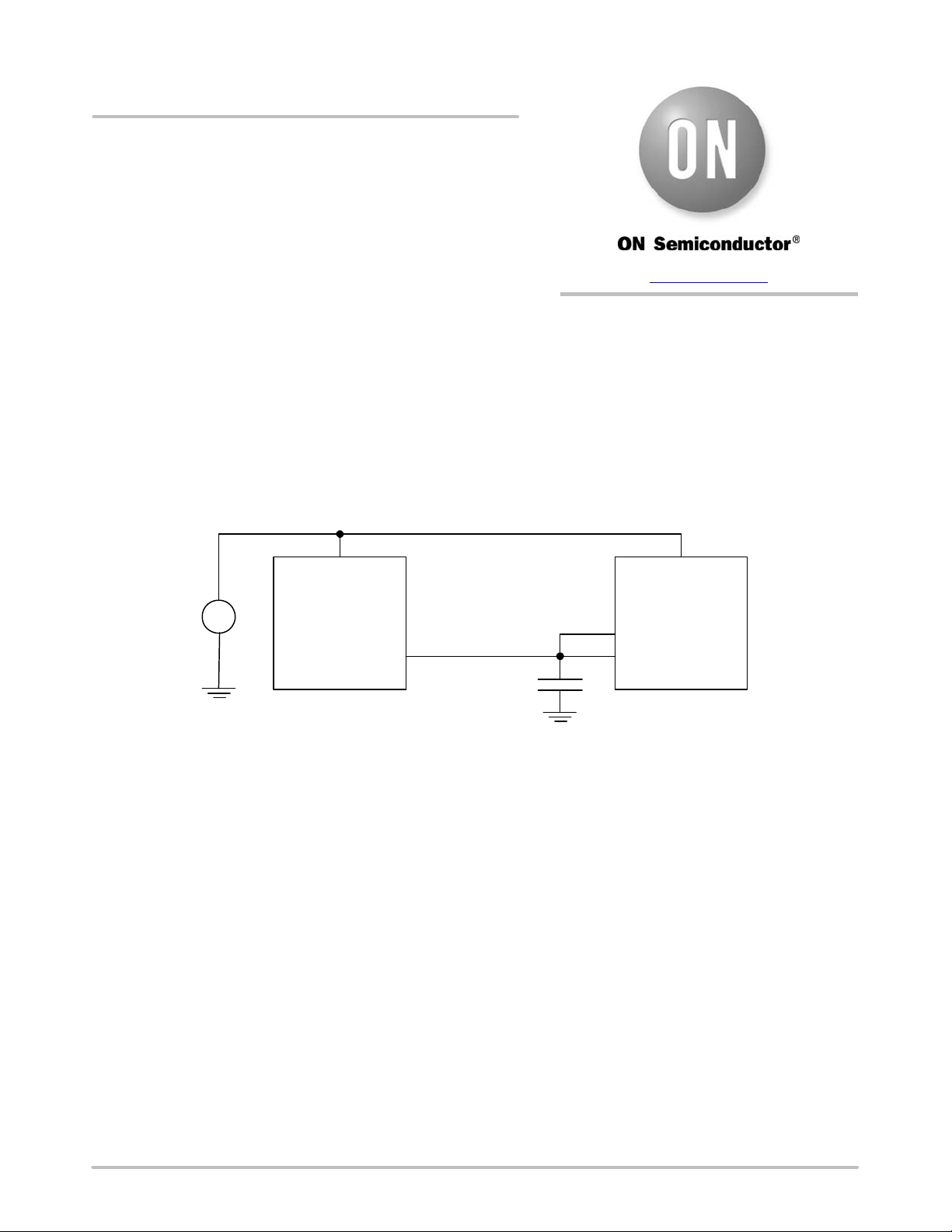
Implementation 1
Connect a digital output pin PIO directly from a
micro−controller to the VREG pin of the RF device. The
default setting of PIO should be Hi−Z.
After powering up the RF device PIO has to be set from
Hi−Z to 1 and back to Hi−Z. This will induce a voltage kick
to VREG and helps the device to power up in minimum time.
Figure 1. Implementation 1
VREG
Microcontroller
PIO
ON Semiconductor
RF device
VDD
C = 1 mF
Powering up references and oscillators should now be
done as follows (see Note):
1. Set PWRMODE to STANDBY (register value
0x05)
2. Set PIO to output 1
3. Wait at least 200 ms
4. Set PIO back to Hi−Z
NOTE: Refer to the product specific Programming
Manual for details on power up sequences, see
http://www.onsemi.com
Implementation 2
This implementation uses a GPIO pin from the RF device
itself, so no extra pin from a micro−controller or any other
external device is required.
Choose a GPIO pin (SYSCLK or IRQ) and connect it via
a capacitor C
2
to the VREG pin. The pin numbers of the
GPIO pins that can be used for each of ON Semiconductor
RF device are shown in Table 1.
www.onsemi.com
APPLICATION NOTE