
下载
© Semiconductor Components Industries, LLC, 2011
October, 2011 − Rev. 0
1 Publication Order Number:
AND8494/D
AND8494/D
Thermal Sensing Methods
used in ON Semiconductor
Devices
Introduction
This application note will describe the standard methods
used by ON Semiconductor devices for temperature
measurement. It will also discuss the various sources of error
that arise and the techniques used to minimize them.
Transistor Basics
For a given collector current, Ic, the basic equation that
relates the temperature of a transistor to the base−emitter
voltage Vbe is:
T:+
q @ Vbe
K @ Ln
ǒ
Ic
Is
Ǔ
(eq. 1)
where:
T is the absolute temperature in degrees Kelvin
K is Boltzmann’s constant (1.38 x 10
−23
JK
−1
)
q is the charge on the electron (1.6 x 10
–19
coulombs)
Ic is the collector current
Is is the reverse saturation current
Theoretically this equation can be used to determine the
transistor temperature by setting Ic and measuring the
base−emitter voltage. In practice this leads to large errors
due to the dependence of the equation on Is, which can vary
widely between transistors. In order to cancel out the
dependency on Is and get a more accurate temperature
measurement, a different technique is required.
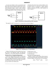
2−Current Sensing Method
The method used to eliminate dependence on Is is to
switch 2 currents through the transistor and measure Vbe for
each one. The difference in Vbe measurements can then be
used to determine the transistor temperature.
Re−arranging Equation 1 to get Vbe gives:
Vbe :+
K @ T
q
@ Ln
ǒ
Ic
Is
Ǔ
(eq. 2)
The difference in Vbe for 2 currents, where Ic1 is the high
level current and Ic2 is the low level current, is:
Vbe1 * Vbe2 :+
K @ T
q
@
ǒ
Ln
ǒ
Ic1
Is
Ǔ
* Ln
ǒ
Ic2
Is
Ǔ
Ǔ
(eq. 3)
which gives:
Vbe1 * Vbe2 :+
K @ T
q
@ Ln
ǒ
Ic1
Ic2
Ǔ
(eq. 4)
Setting Ic1 as a fixed multiple, N, of Ic2 gives:
DVbe :+
K @ T
q
@ Ln(N)
(eq. 5)
This is the equation used internally in 2−current
ON Semiconductor devices to calculate temperature based
on the difference in Vbe measurements. The typical value
used for N is 17. The internal circuitry used in 2−current
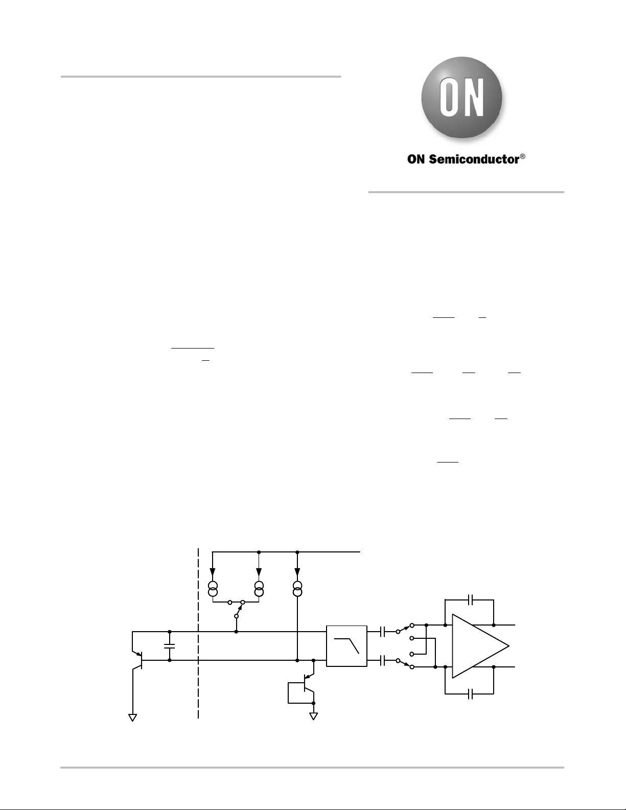
devices is shown in Figure 1.
C1*
D+
I N x 1
D−
REMOTE
SENSING
TRANSISTOR
TO ADC
BIAS
DIODE
LOW−PASS FILTER
Figure 1. Internal Circuit for 2−current Device
* Capacitor C1 is optional. It
is only necessary in noisy
environments.
C1 = 2.2 nF Typ, 3 nF Max.
I
BIAS
V
DD
f
C
= 65 kHz
V
OUT−
V
OUT+
http://onsemi.com
APPLICATION NOTE