
下载

Application Report
SLAA545 – October 2012
1
Interfacing Altera FPGAs to ADS4249 and DAC3482
Matt Guibord High Speed Data Converters
ABSTRACT
Interfacing FPGAs to high speed digital-to-analog converters (DAC) and analog-to-digital converters (ADC)
can be confusing, especially with so many interface formats available. This application note specifically
looks at interfacing Altera FPGAs to the Texas Instrument’s (TI) ADS4249 and DAC3482. Code examples
are provided that are tested and verified using the TSW1400 evaluation platform which interfaces
seamlessly with TI high speed ADCs and DACs. An example of a simple repeater application is shown
which is used as a starting point for a full digital design. The design and timing constraints are discussed in
detail to aid the digital designer in closing timing between the FPGA and the data converters.
Contents
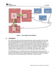
1 Hardware Setup ............................................................................................................................ 2
1.1 TSW1400EVM ........................................................................................................................ 3
1.2 ADS4249EVM ........................................................................................................................ 4
1.3 DAC3482EVM ........................................................................................................................ 4
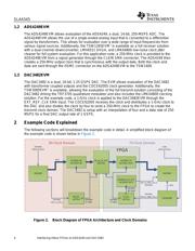
2 Example Code Explained ............................................................................................................. 4
2.1 Input Clocks and Clock Domains ............................................................................................ 5
2.2 Interface Architectures ............................................................................................................ 6
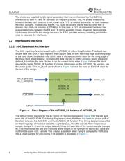
2.2.1 ADC Data Input Architecture ....................................................................................... 6
2.2.2 DAC Data Output Architecture .................................................................................... 9
2.3 Timing Constraints ................................................................................................................ 11
2.3.1 Defining Clocks ......................................................................................................... 12
2.3.2 FPGA Input Timing Constraints ................................................................................. 14
2.3.3 FPGA Output Timing Constraints .............................................................................. 16
2.3.4 Tips for Closing Timing .............................................................................................. 17
3 ADC Interface Without the use of a PLL ................................................................................... 17
4 Conclusion .................................................................................................................................. 18
Figures
Figure 1. Block Diagram of the Hardware ...................................................................................... 3
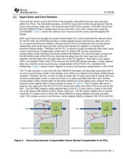
Figure 2. Block Diagram of FPGA Architecture and Clock Domains ........................................... 4
Figure 3. Source-Synchronous Compensation Versus Normal Compensation in ALTPLL .......
5
Figure 4. Block Diagram of the ALTDDIO_RX Instance of ALTDDIO_IN ...................................... 6
Figure 5. Default ALTDDIO_IN Timing Diagram............................................................................. 7
Figure 6. ALTDDIO_IN Timing Diagram with Inverted clockin ...................................................... 8
Figure 7. Arrangement and Reordering of ADC Bits out of the ALTDDIO_IN Function .............. 9
Figure 8. Block Diagram of the ALTDDIO_TX Instance of ALTDDIO_OUT .................................. 9
Figure 9. Block Diagram of the ALTDDIO_CLK_OUT Instance of ALTDDIO_OUT .................... 10
Figure 10. Timing Diagram of ALTDDIO_TX and ALTDDIO_CLK_OUT ........................................ 11
Figure 11. Default Setup and Hold Times for the ADS4249 with a 250-MHz Clock ..................... 13
Figure 12. Timing Requirements from the ADS4249 Datasheet ................................................... 14
Figure 13. SDC Input Timing Constraints Illustrated .................................................................... 15