


下载

AN-638
APPLICATION NOTE
One Technology Way • P.O. Box 9106 • Norwood, MA 02062-9106 • Tel: 781/329-4700 • Fax: 781/326-8703 • www.analog.com
INTRODUCTION
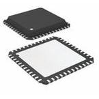
This application note describes the 32-lead ADN2847
laser diode driver Rev. A1 evaluation kit. The evaluation kit
is a demonstration board that provides ac-coupled opti-
cal evaluation of the ADN2847. This document describes
how to congure the board to operate these parts opti-
cally. The document contains the following information:
• Board description
• Quick start for optical operation
• Description of board settings
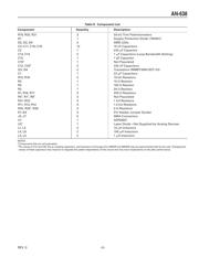
• Component list
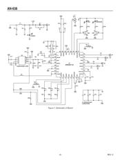
• Schematic of board
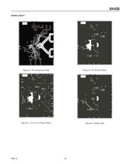
• Board layout Information
• Silkscreen image of board
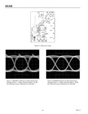
• Optical eyes
BOARD DESCRIPTION
The ADN2847 is a 3 V dual-loop 50 Mbps to 3.3 Gbps laser
diode driver. To use the board in an optical conguration,
a suitable laser diode must be soldered onto the board.
The monitor photodiode (MPD) current is fed into the
ADN2847 to control the average power and extinction
ratio. The ADN2847 uses automatic power control (APC)
to maintain a constant average power over time and tem-
perature. The ADN2847 uses closed-loop extinction ratio
control to allow optimum setting of the extinction ratio for
every device. This board is congured for lasers in mini-
DIL packages only. LEDs for power supply, DEGRADE, and
FAIL are made available for monitoring purposes. Power
to the ADN2847 evaluation circuitry is –3.3 V only.
QUICK START FOR OPTICAL OPERATION
To ensure proper operation in the optical conguration,
verify the following:
1. Jumpers K3 and K4 are connected to A; Jumper K2 is
connected to B.
2. If the input data is clocked, it is necessary to enable
the clock select pin (CLKSEL). CLKSEL is enabled by
connecting K4 to B. If the clock inputs are not used,
or the input data is not latched, connect K4 to A.
ADN2847 AC-Coupled Optical Evaluation Kit
By Mark Murphy, Ferenc Barany, and Michael O’Flanagan
3. The power supply is diode protected to ensure the
device is not damaged if a positive power supply is
accidently connected. The user may connect Jumper
K1 (short circuit) and power up the board by applying
–3.3 V to the power input SMA, J3. If Jumper K1 is not
connected, the user should make the power supply
sufciently negative to ensure that the ADN2847 sup-
ply is –3.3 V. The actual DUT supply can be measured
at the anode of D1.
4. Apply a differential signal, typically 500 mV, to J6 and
J7 (DATAN and DATAP). Single-ended operation may
result in a degraded eye.
5. If the clock select pin is enabled by K4, apply a
differential clock signal, typically 500 mV, to J4 and
J5 (CLKN and CLKP). If the clock pin is not enabled,
a clock signal should not be connected.
6. The optical eye and switching characteristics of the
ADN2847 may be observed using a digital communi-
cations analyzer that has an optical input channel with
the required bandwidth.
7. The bias and modulation currents can also be moni-
tored by observing IBMON and IMMON, respectively.
IBMON and IMMON are both a 1:100 ratio of I
BIAS
and
IMOD. Both are terminated with resistors and so can
be viewed at Test Points T3 and T4 using a voltmeter
or oscilloscope.
8. To establish the desired average power and extinction
ratio, the user should follow this procedure.
a. With the power supply turned off, adjust Potentiom-
eters R20 (ERSET) and R21 (PSET) to approximately
20 k.
b. With the evaluation board powered on and the data
signal switching, the user can reduce the value of
Potentiometer R21 to establish the desired average
optical power.
c. Potentiometer R20 can then be reduced in value
to increase the modulation current and hence
increase the extinction ratio. The bias and modula-
tion currents can be monitored using IBMON and
IMMON.
REV. 0