
下载
REV. PrA May 20, 2002
Information furnished by Analog Devices is believed to be accurate and
reliable. However, no responsibility is assumed by Analog Devices for its
use, nor for any infringements of patents or other rights of third parties
which may result from its use. No license is granted by implication or
otherwise under any patent or patent rights of Analog Devices.
a
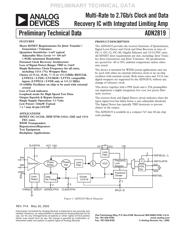
Preliminary Technical Data ADN2819
One Technology Way, P.O. Box 9106, Norwood, MA 02062-9106, U.S.A.
Tel: 781/329-4700 www.analog.com
Fax: 781/326-8703 © Analog Devices, Inc., 2002
Multi-Rate to 2.7Gb/s Clock and Data
Recovery IC with Integrated Limiting
Amp
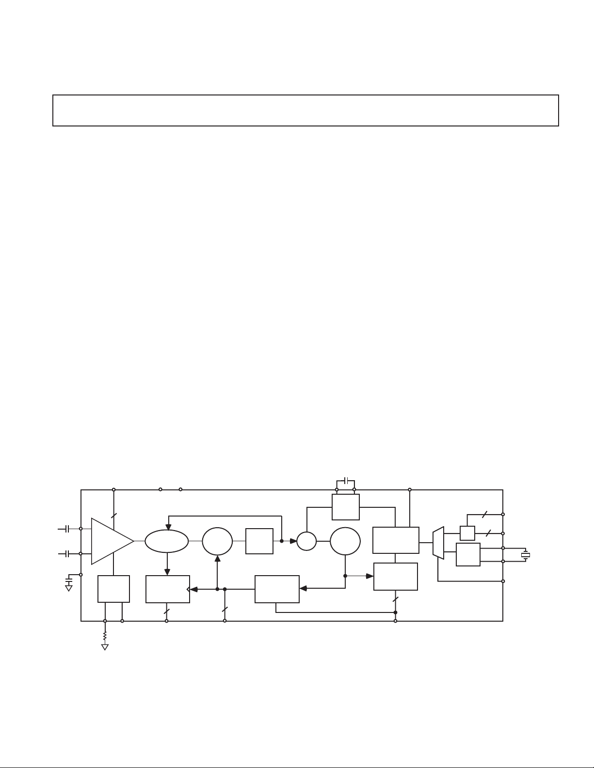
Figure 1. ADN2819 Block Diagram
Level
Detect
Quantizer
2
SLICEP/N
PIN
NIN
Phase
Shifter
Phase
Det.
Loop
Filter
Σ
VCO
Data
Re-Timing
Divider
1/2/4/16
Loop
Filter
2
2
Fractional
Divider
XTAL
Osc
Frequency
Lock
Detector
3
CF1
CF2
LOL
/n
REFSEL
2
REFSEL[0..1]
2
REFCLKP/N
XO1
XO2
SEL[0..2]
THRADJ SDOUT DATAOUTP/N CLKOUTP/N
VREF
VCC
VEE
FEATURES
Meets SONET Requirements for Jitter Transfer /
Generation / Tolerance
Quantizer Sensitivity: 4 mV typical
Adjustable Slice Level: +/- 100 mV
1.9GHz minimum Bandwidth
Patented Clock Recovery Architecture
Loss of Signal Detect Range: TBD to 15mV
Single Reference Clock Frequency for all rates,
including 15/14 (7%) Wrapper Rate
Choice of 19.44, 38.88, 77.76 or 155.52MHz REFCLK.
LVPECL / LVDS / LVCMOS / LVTTL compatible
inputs (LVPECL / LVDS only at 155.52 MHz)
19.44MHz Oscillator on chip to be used with external
crystal
Loss of Lock indicator
Loopback mode for High Speed Test Data
Output Squelch & Bypass features
Single Supply Operation: 3.3 Volts
Low Power: 540mW Typical
7 x 7 mm 48 pin LFCSP
APPLICATIONS
SONET OC-3/12/48, SDH STM-1/4/16, GbE and 15/14
FEC rates
WDM Transponders
Regenerators/Repeaters
Test Equipment
Backplane Applications
PRODUCT DESCRIPTION
The ADN2819 provides the receiver functions of Quantization,
Signal Level Detect and Clock and Data Recovery at rates of
OC-3, OC-12, OC-48, Gigabit Ethernet and 15/14 FEC rates.
All SONET jitter requirements are met, including: Jitter Trans-
fer; Jitter Generation; and Jitter Tolerance. All specifications
are quoted for -40 to 85C ambient temperature unless other-
wise noted.
The device is intended for WDM system applications and can
be used with either an external reference clock or an on-chip
oscillator with external crystal. Both native rates and 15/14 rate
digital wrappers are supported by the ADN2819, without any
change of reference clock.
This device together with a PIN diode and a TIA preamplifier
can implement a highly integrated, low cost, low power fiber
optic receiver.
The receiver front end Signal Detect circuit indicates when the
input signal level has fallen below a user adjustable threshold.
The Signal Detect has typically TBD hysteresis to prevent
chatter at the output.
The ADN2819 is available in a compact 7x7 mm 48 pin chip
scale package.
PRELIMINARY TECHNICAL DATA
页面指南