

下载
AN-636
APPLICATION NOTE
One Technology Way • P.O. Box 9106 • Norwood, MA 02062-9106, U.S.A. • Tel: 781.329.4700 • Fax: 781.461.3113 • www.analog.com
Rev. A | Page 1 of 8
ADN2819 Evaluation Board
by Kevin Buckley
INTRODUCTION
This application note describes the use of the ADN2819
evaluation board. The ADN2819 is a multirate clock recovery,
data-retiming device based on a multiloop PLL architecture.
The ADN2819 can recover clock and data at SONET OC-3,
OC-12, OC-48, and Gigabit Ethernet data rates as well as 15/14
Forward Error Correction (FEC) for these rates by using a
single reference clock or external crystal oscillator.
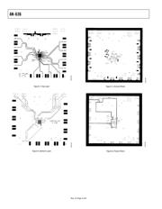
The ADN2819 evaluation board is fabricated using standard
FR-4 materials. All high speed signal traces are matched to
within 1 mil length and maintain a 50 Ω characteristic
impedance to preserve signal integrity. The ADN2819
evaluation board is also used for the
ADN2811.
QUICK START GUIDE FOR OC-48, NORMAL
OPERATING MODE
1. Apply a 3.3 V supply to the AVCC and GND vector pins.
2. Connect PIN/NIN to a pattern generator that can supply a
differential input of greater than 10 mV to the ADN2819.
Use cables of matching length.
3. Connect CLKOUTP/CLKOUTN, DATAOUTP/
DATAOUTN to measurement equipment using cables of
matching length.
4. All switches, S1 through S9, should be in the 0 position.
1
This sets the part up in OC-48, normal operating mode,
using the on-board 19.44 MHz crystal as the reference
clock.
5. Apply a single-ended or differential 2.488 Gbps NRZ data
stream to the ADN2819 inputs. The recovered 2.488 GHz
clock and retimed data is present at the CLKOUTP/
CLKOUTN and DATAOUTP/DATAOUTN outputs,
respectively.
1
For a 0, the red switch should be in the right-most position, as shown in
Figure 1. For the ADN2819 evaluation boards that are populated with 3-pin
jumpers instead of the slide switches, the jumper should be placed on the
left-most two pins for a 0.
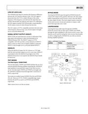
03563-001
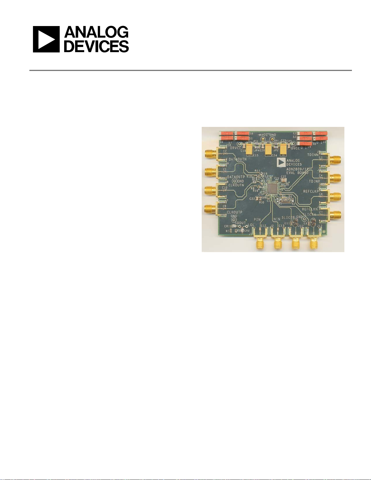
Figure 1. ADN2819 Evaluation Board (Actual Size)
POWER SUPPLY
The ADN2819 evaluation board requires a single 3.3 V nominal
supply for basic operation. This supply is brought on-board
through vector pins AVCC and GND at the top center of the
board. The evaluation board is shipped configured for a single
supply through Jumpers JP1 through JP4, which are populated
with ferrite beads. If these ferrite beads are removed, separate
3.3 V supplies must be applied to vector pins DVCC and
DRVCC. This allows the user to keep the analog supply, digital
supply, and output driver supply separate, although it is not
required.
DATA RATE SELECTION
The input data rate of the ADN2819 is selected by SEL0, SEL1,
SEL2, Switches S2 through S4 (see
Table 1 ). The ADN2819 can
be programmed to acquire OC-3 (155.52 Mbps), OC-3 FEC
(166.6 Mbps), OC-12 (622.08 Mbps), OC-12 FEC (666.5 Mbps),
OC-48 (2.488 Gbps), OC-48 FEC (2.665 Gbps), Gigabit
Ethernet (1.25 Gbps), and Gigabit Ethernet FEC (1.339 Gbps).