


下载
AN-924
APPLICATION NOTE
One Technology Way • P. O. Box 9106 • Norwood, MA 02062-9106, U.S.A. • Te l: 781.329.4700 • Fax: 781.461.3113 • www.analog.com
Digital Quadrature Modulator Gain
by Ken Gentile
Rev. 0 | Page 1 of 4
INTRODUCTION
Digital quadrature modulators appear in a number of commu-
nications and signal processing ICs. This application note
explains the basic building blocks of a digital quadrature
modulator, along with an analysis of the gain through the
modulator for three types of input signals.
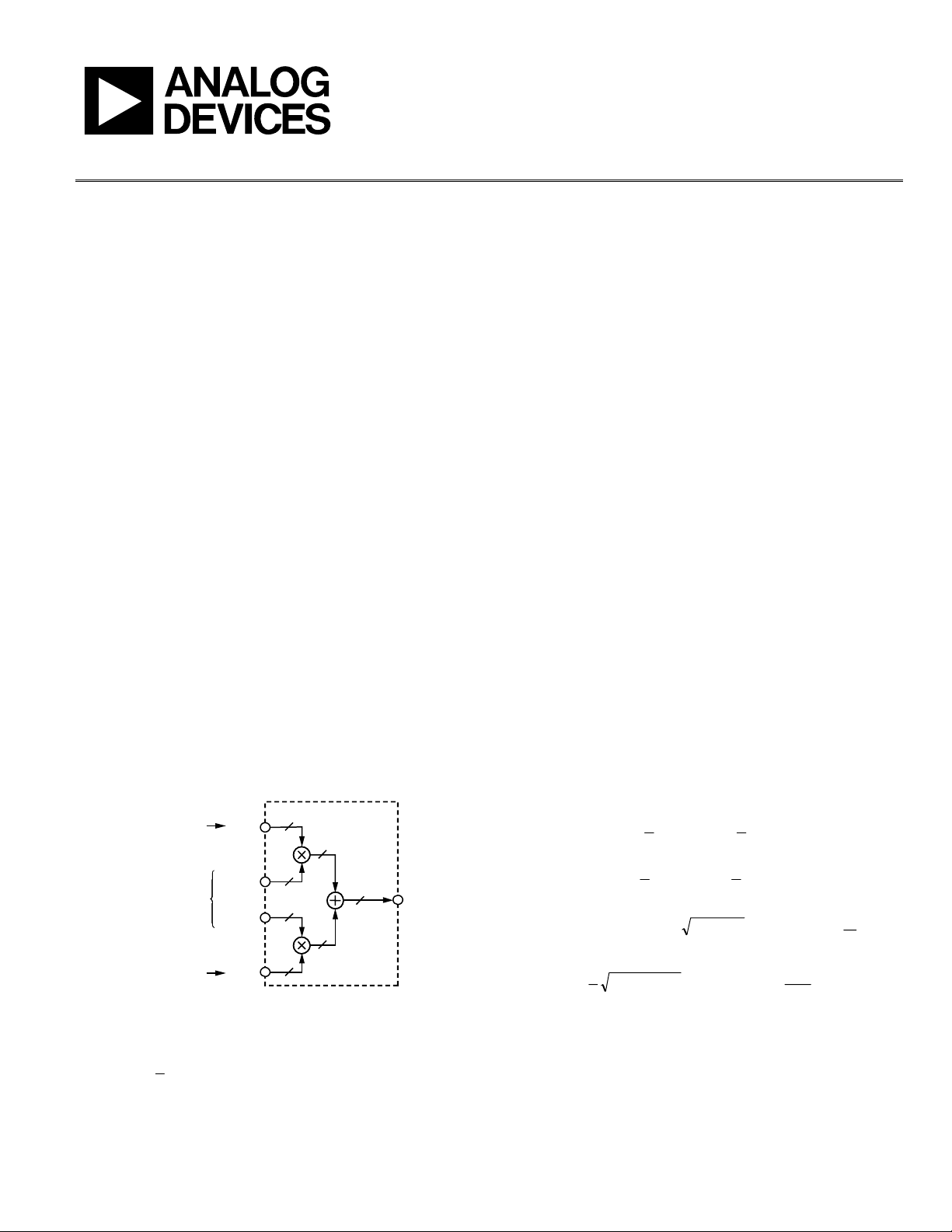
The generic digital modulator consists of a pair of digital
multipliers and a digital adder, configured as shown in
Figure 1.
Generally, the binary numbers associated with the data paths all
have the same numeric range, namely ±1. This applies to the
input (I, Q, and carrier), output (Y), and intermediate data
paths. An N-bit bus width is shown in the diagram for the sake
of generality, where the N bits represent fractional numeric
values between ±1. Of the four inputs, two are dedicated to
processing the digital carrier signal, which is an N-bit quantized
representation of the sine and cosine waves that constitute a
quadrature carrier. By definition, the carrier has separate cosine
and sine components, both of which oscillate (numerically) at
radian frequency, ω
C
(where ω
C
equates to 2πf
C
, with f
C
denoting
the more familiar units of sinusoidal frequency). The other two
inputs (I and Q) are used for processing a digital, N-bit quantized,
baseband signal. The I and Q labels are shorthand notation for
the in-phase and quadrature components, respectively, of the
baseband signal. The output, Y, is an N-bit quantized digital
representation of the baseband signal upconverted to the carrier
frequency (f
C
).
I
sin(ω
c
t
)
cos(ω
c
t
)
Y
Q
QUADRATURE
CARRIER SIGNAL
IN-PHASE
INPUT SIGNAL
DIGITAL
QUADRATURE
MODULATOR
QUADRATURE
INPUT SIGNAL
N
N
N
N
N
N
N
–
06830-001
Figure 1. Digital Quadrature Modulator Functional Diagram
The relationship between the input and output signals may be
expressed as a function of time, as shown in Equation 1.
[]
(1)
The carrier signal is time dependent by definition as indicated
by the t term in the arguments of the sine and cosine functions.
The Y, I, and Q terms have been assigned t arguments as well,
indicating that their values can also be time dependent. The
scale factor of ½ is a consequence of using the same number of
bits at both the input and output of the adder. Note that the sum
of the two N-bit multiplier outputs actually requires N + 1 bits
to represent the full range of the summed results. However, the
act of constraining the output of the adder to only N bits means
that the least significant bit of the N + 1 bit result must be
discarded. The act of truncating the sum to N bits results in an
intrinsic 50% loss through the adder, hence the scale factor of ½
that appears in Equation 1.
An analysis of the output signal, Y(t), for three different types of
I and Q input signals follows. The input signal types under
consideration are:
1. A static input signal
2. A nonquadrature sinusoidal input signal
3. A quadrature sinusoidal input signal
The following analysis is aided by the trigonometric identities
given by Equation 2 and Equation 3. In addition, the formula
given in Equation 4 is useful for quadrature signal analysis. It
relates a quadrature expression (the left side) to a cosine func-
tion (the right side). Of particular interest is the application of
Equation 4 to Equation 1, which produces an alternate form for
Y(t), as shown in Equation 5.
)cos(
2
1
)cos(
2
1
)cos()cos( yxyxyx −++=
(2)
)cos(
2
1
)cos(
2
1
)sin()sin( yxyxyx +−−=
(3)
⎥
⎦
⎤
⎢
⎣
⎡
⎟
⎠
⎞
⎜
⎝
⎛
+=±
A
B
xBAxBxA arctancos)sin()cos(
22
m
(4)
⎥
⎥
⎦
⎤
⎢
⎢
⎣
⎡
⎟
⎟
⎠
⎞
⎜
⎜
⎝
⎛
++=
)(
)(
arctancos)()(
2
1
)(
22
tI
tQ
tωtQtItY
C
(5)
)sin()()cos()(
2
1
)( tωtQtωtItY
CC
−=