


下载
AN-589
Application Note
One Technology Way • P. O. Box 9106 • Norwood, MA 02062-9106, U.S.A. • Tel: 781.329.4700 • Fax: 781.461.3113 • www.analog.com
Ways to Optimize the Performance of a Difference Amplifier
by Reza Moghimi
Rev. B | Page 1 of 4
There are times when a small signal needs to be measured in
the presence of a large common-mode signal. Traditional
instrumentation amplifiers (in-amps) that have two op amp or
three op amp internal configurations are commonly used in
these applications. Although in-amps have good common-mode
rejection ratios (CMRR), price and sometimes specifications
prevent their usage in these applications. In-amps may not have
the right bandwidth, dc accuracy, or power consumption
requirements that the user requires. Therefore, in these situations,
users build their own difference amplifiers by using a single
amplifier and external resistors as an alternative to instrumentation
amplifiers. Unless a set of tightly matched resistors is used, CMRR
of these circuits are very low. This application note presents
several ways to build and optimize the performance of a discrete
difference amplifier. It also recommends amplifiers that make
the overall solution cost/performance competitive with monolithic
instrument amplifiers.
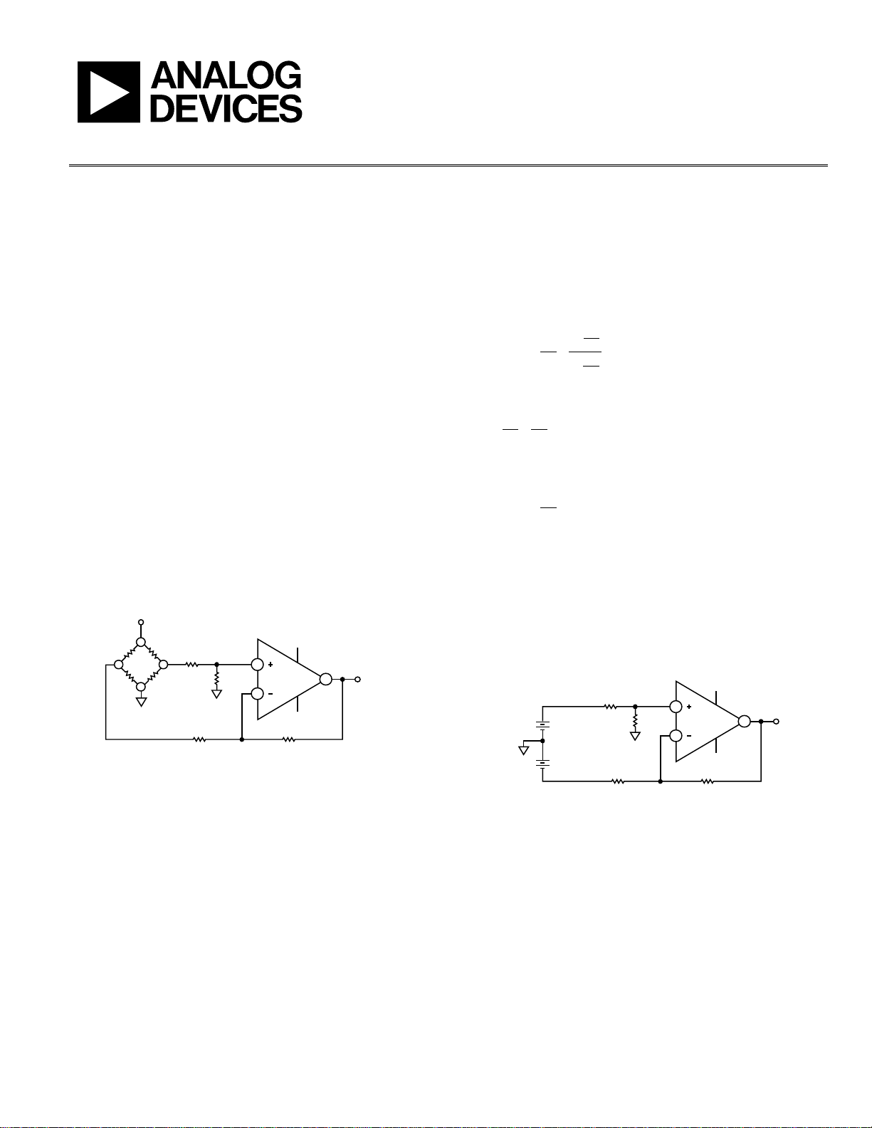
A typical difference amplifier using a single amplifier connected
to a sensor bridge is shown in Figure 1.
2
1
3
R3
R4
U8
V
REF
AOZ
AO1
V
OUT
V+
V–
4
21
3
0
0
R1 R2
02867-001
Figure 1.
By applying the superposition principle, it can be shown that
the output is a function of the difference of the two inputs. The
transfer function of the circuit in Figure 1 is:
−
+
+
= 12
4
3
1
2
1
1
1
2
VV
R
R
R
R
R
R
V
OUT
(1)
A special situation arises when
4
3
2
1
R
R
R
R
=
and Equation 1 is reduced to
( )
12
1
2
VV
R
R
V
OUT
−=
(2)
The output is the difference of the two inputs times a gain factor
that can be set to unity. Equation 2 holds true if the ratio of the
resistors is tightly matched. Assuming perfectly matched resistors
with values of R2 = R4 = 10 kΩ, R1 = R3 = 1 kΩ, V1 = 2.5 V,
V2 = 2.6 V, then V
OUT
= 1 V.
As stated above, one of the shortcomings of the circuit in Figure 1 is
the poor CMRR, which is caused by mismatch of the resistors.
To investigate this, the circuit is redrawn for clarity in Figure 2.
2
1
3
R3
BR4
R4
V
REF/2
+ V
D/2
V
REF/2
– V
D/2
U9
V
OUT
V+
V–
R1
R2
(1-ERROR)
02867-002
0
0
BRIDGE
+
–
+
–
Figure 2.