下载

AN-756
APPLICATION NOTE
One Technology Way • P.O. Box 9106 • Norwood, MA 02062-9106 • Tel: 781/329-4700 • Fax: 781/326-8703 • www.analog.com
Sampled Systems and the Effects of Clock Phase Noise and Jitter
by Brad Brannon
ABSTRACT
As higher resolution data converters capable of direct
IF-sampling come to market, system designers need help
making performance/cost trade-off decisions on low jit-
ter clock circuits. Many of the traditional methods used to
specify clock jitter are not applicable to data converters
or at best reveal only a fraction of the story. Without a
proper understanding of how to specify and design the
clocking circuit, optimal performance of these new data
converters may not be achieved. A simple jitter speci-
cation is rarely sufcient for making an informed clock
selection. Rather, it is important to know the bandwidth
and spectral shape of the clock noise so that this can
be properly accounted for during the sampling process.
Today many system designers are not adequately speci-
fying the phase noise and jitter requirements for the data
converter clock and, as a result, system performance is
degraded. Picoseconds of clock jitter quickly translate
to dBs lost in the signal path. However, in the opposite
extreme, some designers may be paying too much for an
expensive clock source simply because they are unclear
on how clock noise affects the converter and ultimately
their product’s performance. Note that the most ex-
pensive clock generator does not always yield the best
system performance. This application note explains
many of the trade- offs related to jitter, phase noise,
and converter performance. Once these trade-offs are
understood, the best clock for the application may be
selected and optimal performance at the lowest cost will
result. After explaining how the sampling process works
in a data converter, real application examples are given
to illustrate the clock selection process.
HISTORY
One of the issues that arises most often regarding ADC
applications is that of providing an encode source. As
most engineers are aware, proper selection of the encode
clock is most critical in attaining the best performance
from the selected data converter. This is especially true
with the sampled analog input frequencies continuing to
increase as seen in recent years.
However, as the converters have moved closer to the
antenna in these signal chains, the engineers using
them have moved from the “mixed signal designer”
to the “RF designer.” Likewise, the design techniques
and supporting components have also changed and
the focus has shifted from time domain characteristics
to frequency characteristics. In past times, the encode
clock was just that—a clock. For IF and RF sampling
systems, the encode source is now considered more
of a local oscillator than a clock for reasons discussed in
this application note. As such, many designers expect
clock requirements to be specied in the frequency
domain, just as they are for RF synthesizers.
While it is difcult to provide for direct correlation
between clock jitter and phase noise, this application
note provides some guidelines for designing or
selecting encode sources from either a clock jitter
or phase noise perspective. There are a number of
articles available on translating between phase noise
and jitter, and this application note may be useful in the
validation of the process.
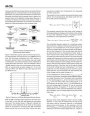
JITTER DEFINED
Since the primary purpose of a data converter is to take
regular time samples and produce an analog, or to take
an analog continuum and produce a series of regular time
samples, stability of the sampling clock is very impor-
tant. From a data converter perspective, this instability
is called clock jitter and results in uncertainty as to when
the analog input is actually sampled. Although there are
several methods to measure clock jitter directly, as the
clock stability requirements tighten up the requirement
to measure sub -picosecond timing variations dictate
that indirect measurement be used. From a converter
perspective, note that the encode bandwidth can extend
over many hundreds of MHz. Therefore, when consid-
ering the bandwidth of the noise that constitutes jitter
for a data converter, the range is from dc to the encode
bandwidth that exceeds far beyond the typical 12 kHz to
20 MHz numbers often quoted for standard clock jitter
measurements.
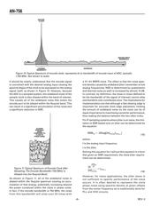
Since the concern with jitter is reduced wideband con-
verter noise performance, it is easy to estimate clock
jitter by observing the degradation in noise performance
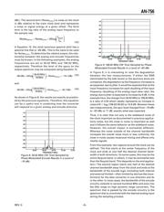
of a converter. SNR limitations due to jitter can be deter-
mined by the following equation:
SNR 20log 2 f t dB
analog
jitter
rms
= −
( )
π
(1)
REV. 0

