
下载

AN-691
APPLICATION NOTE
One Technology Way • P.O. Box 9106 • Norwood, MA 02062-9106 • Tel: 781/329-4700 • Fax: 781/461-3113 • www.analog.com
Operation of RF Detector Products at Low Frequency
by Matthew Pilotte
INTRODUCTION
Analog Devices has many RF detector products in its
portfolio designed to operate over various frequency
ranges up to 8.0 GHz. Most of these parts can also
perform very well at frequencies down into the audio
band, although the data sheets for these parts list
performance and specify guaranteed operation at much
higher frequencies. The low input frequency performance
of these parts is summarized in this application note. Plots
of performance are included.
The low frequency performance of the following parts
is discussed in this application note: AD8302, AD8306,
AD8307, AD8309, AD8310, AD8361, and AD8362. (The
AD8314 is not included because it contains a series
capacitor at its input, which precludes its use at low
frequency.) Using the appropriate precautions, some
of these devices can be dc-coupled at their inputs. The
external circuitry substantially determines the lowest
frequency at which operation is acceptable.
These devices can be grouped into four general catego-
ries: demodulating logarithmic ampliers, exponential
logarithmic ampliers, special purpose circuits employ-
ing demodulating logarithmic ampliers, and rms-to-dc
converters. Table I shows the category into which each
part falls.
Table I.
Part Number Category
AD8302 Special Purpose
AD8306 Demodulating Logarithmic Amplier
AD8307 Demodulating Logarithmic Amplier
AD8309 Demodulating Logarithmic Amplier
AD8310 Demodulating Logarithmic Amplier
AD8361 RF rms-to-dc Converter
AD8362 Exponential Logarithmic Amplier
It is important to understand each of the fundamental
performance parameters for these categories of parts.
The data sheet for each device includes a comprehensive
theory of operation section that goes into detail beyond
what is presented here.
Demodulating Logarithmic Ampliers
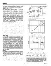
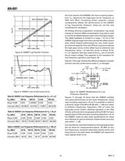
ADI’s demodulating logarithmic ampliers (log amps)
produce an output that is proportional to the common
logarithm of the input signal amplitude; this response
is described as being linear-in-dB. The transfer function
produced is a straight line when plotted against the input
signal magnitude, expressed in decibels. This straight line is
described in ADI data sheets by its slope and its x intercept.
Because these log amps are very sensitive, the response
to the tiny amount of noise that is inevitably generated in
the input sections of the log amps is indistinguishable at
the detector output from the response to very small input
signals. Consequently, the detected output voltage typically
does not go to 0 V when the amplitude of the input signal
goes to 0 V, but reaches a lower limit that is typically in the
sub-300 mV range as the input signal amplitude nears 0 V.
The x intercept discussed here is the extrapolated point at
which the transfer function would intersect the horizontal
axis, if it were capable of doing so. See Figure 1.
The slope of the transfer function is simply the change
in the detected output voltage over the change in input
signal amplitude, expressed in dB. For log amps, slope is
expressed in terms of millivolts per dB.
Both of these values are determined by performing a
linear regression over the straightest central portion of
the actual detected output voltage versus input signal
level curve. Then, the actual measured voltage at each
input level is compared to that predicted by the linear
regression to determine the law conformance of the part.
The law conformance of an ideal log amp versus input
signal level is 0 dB. In practice, the dynamic range of ADI
log amps is typically dened to be the range over which
the law conformance is ±1 dB maximum.
Figure 1. Basic Log Amp Transfer Function
REV. 0