

下载
REV. 0
a
AN-592
APPLICATION NOTE
One Technology Way • P.O. Box 9106 • Norwood, MA 02062-9106 • Tel: 781/329-4700 • Fax: 781/326-8703 • www.analog.com
© Analog Devices, Inc., 2002
Recommendations for the Use of the CONVST Input
of the AD7822/AD7825/AD7829 and the AD7827
by Sally Paterson
INTRODUCTION
The AD7822/AD7825/AD7829 are high speed 1-, 4-, and
8-channel parallel 8-bit ADCs, and the AD7827 is a high
speed, single-channel, serial 8-bit ADC. They are all half
flash ADCs with similar functionality of the CONVST
input. This Application Note describes some consider-
ations that are worth noting with the CONVST input and
recommendations for avoiding any application issues.
FUNCTION OF THE CONVST INPUT
The CONVST signal is an input to the devices. It is used
to power up the devices, initiate conversions, and place
the devices into the Power-Down Mode.
A falling edge on CONVST places the track-and-hold into
hold mode and thus initiates an 8-bit analog-to-digital
conversion. The track-and-hold goes back into track
120 ns after the start of the conversion. The state of the
CONVST signal is checked at the end of a conversion,
and if it is logic low, the devices will power down. If in
power-down, a rising edge on CONVST will power up
the devices.
CONVST INPUT TROUBLESHOOTING
When V
DD
is first applied, the devices are in a low
current mode of operation. These devices therefore
need to be powered up before conversions can be initi-
ated. This is done by applying a rising edge to the
CONVST pin. It is important that V
DD
is stable before this
rising edge is applied. If CONVST rises before V
DD
has
settled, or if it goes above V
DD
while it is rising, the
devices will attempt to power up but will fail to do so
properly. Subsequently, when CONVST then goes low
either by bringing it low to initiate a conversion or by the
falling edge of a glitch on the line, the devices will fail to
convert correctly. This is due to conversions being initi-
ated with the devices not being powered up properly.
This can cause the devices to lock up and will result in
no end of conversion (EOC) signal being returned by the
particular device, meaning it has failed to convert cor-
rectly. If this occurs, the recovery method is to perform a
power cycle while ensuring CONVST does not rise before V
DD
.
RECOMMENDATIONS
Ideally, to avoid any issues, CONVST should either be
maintained low until V
DD
has settled or remain at a lower
voltage than V
DD
while it is rising. It should also never be
floating once V
DD
is applied. If this cannot be guaran-
teed, then it is recommended that the CONVST input be
forced to track the V
DD
voltage but never rise above it.
This is achieved by connecting a 10 k⍀ pull-up resistor
and a Schottky diode in parallel, between CONVST and
V
DD
. By doing this, CONVST will never rise before V
DD
nor glitch when V
DD
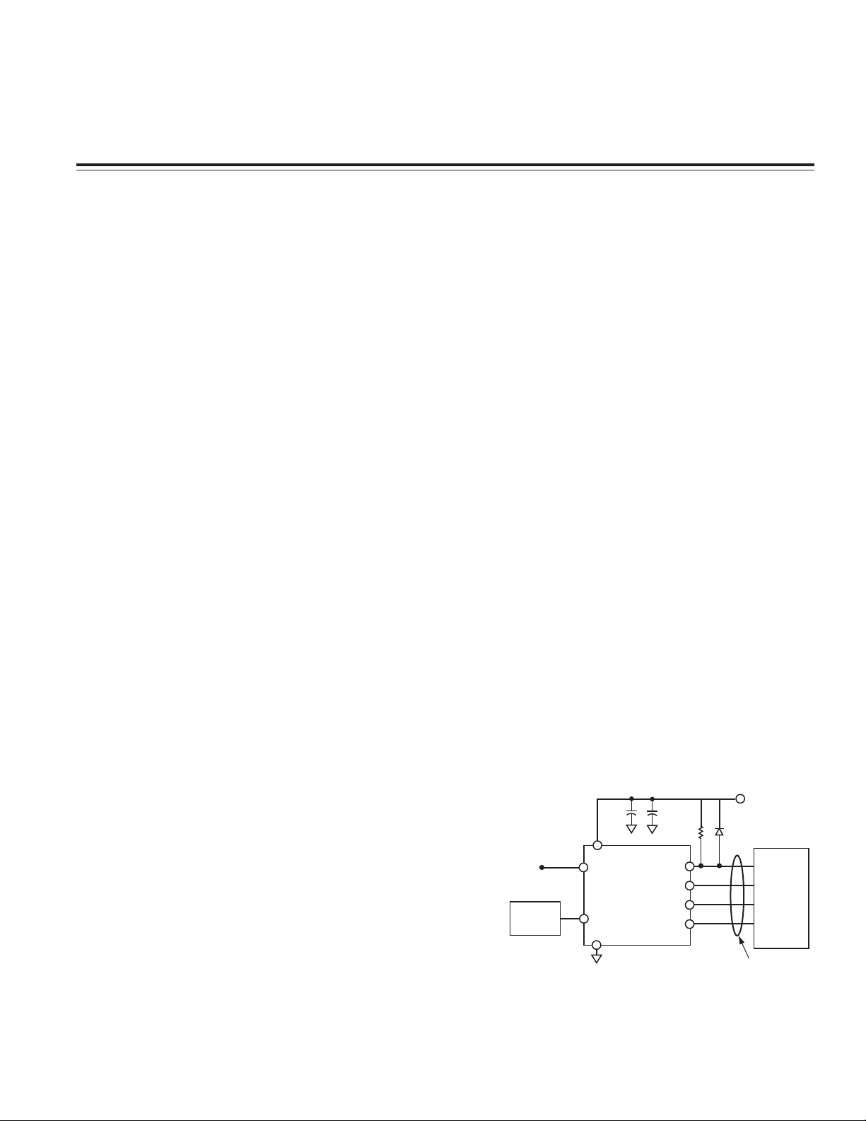
is rising. Figure 1 shows a typical
connection diagram for the AD7827 (the CONVST con-
nection in this diagram also applies to the AD7822/
AD7825/AD7829 parallel devices).
It is important to also note that CONVST (or any other
inputs to the devices) should never be applied before
V
DD
because by doing so the maximum ratings of the particular
device will be exceeded resulting in possible permanent
damage. See the Absolute Maximum Ratings of the
particular data sheet for more detailed information.
AD7827
2.5V
AD780
0V TO 2.5V (V
DD
= 5V)
0V TO 2V (V
DD
= 3V)
INPUT
C/P
V
DD
V
IN
V
REF
3V ⴞ10% OR
5V ⴞ10%
CONVST
SCLK
D
OUT
RFS
GND
10F
SERIAL
INTERFACE
0.1F
SCHOTTKY
DIODE
10k⍀
Figure 1. Typical Connection Diagram of the AD7827
E02971–0–6/02(0)
PRINTED IN U.S.A.