
下载
74LVC2G06
Document number: DS35161 Rev. 6 - 2
1 of 13
www.diodes.com
March 2015
© Diodes Incorporated
74LVC2G06
DUAL INVERTERS with OPEN DRAIN OUTPUTS
Description
The 74LVC2G06 is a dual inverter gate with open drain outputs. The
device is designed for operation with a power supply range of 1.65V
to 5.5V. The input is tolerant to 5.5V allowing this device to be used
in a mixed voltage environment. The device is fully specified for
partial power down applications using I
OFF
. The I
OFF
circuitry disables
the output preventing damaging current backflow when the device is
powered down. The open-drain output can be connected to other
open drain outputs to implement active-low wired-OR or active-high
wired-AND functions. The maximum sink current is 32mA.
Features
Wide Supply Voltage Range from 1.65V to 5.5V
-24mA Output Drive at 3.0V
CMOS Low Power Consumption
IOFF Supports Partial-Power-Down Mode Operation
Inputs Accept up to 5.5V
ESD Protection Tested per JESD 22
Exceeds 200-V Machine Model (A115)
Exceeds 2000-V Human Body Model (A114)
Exceeds 1000-V Charged Device Model (C101)
Latch-Up Exceeds 100mA per JESD 78, Class I
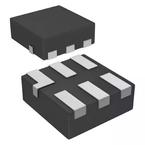
DFN1409 package designed as a direct replacement for chip
scale packaging.
Range of Package Options SOT26, SOT363, X1-DFN1010-6,
X2-DFN1010-6, X2-DFN1409-6, and X2-DFN1410-6
Leadless Packages Named per JESD30E
Totally Lead-Free & Fully RoHS Compliant (Notes 1 & 2)
Halogen and Antimony Free. “Green” Device (Note 3)
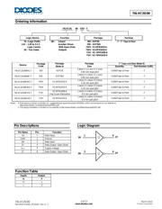
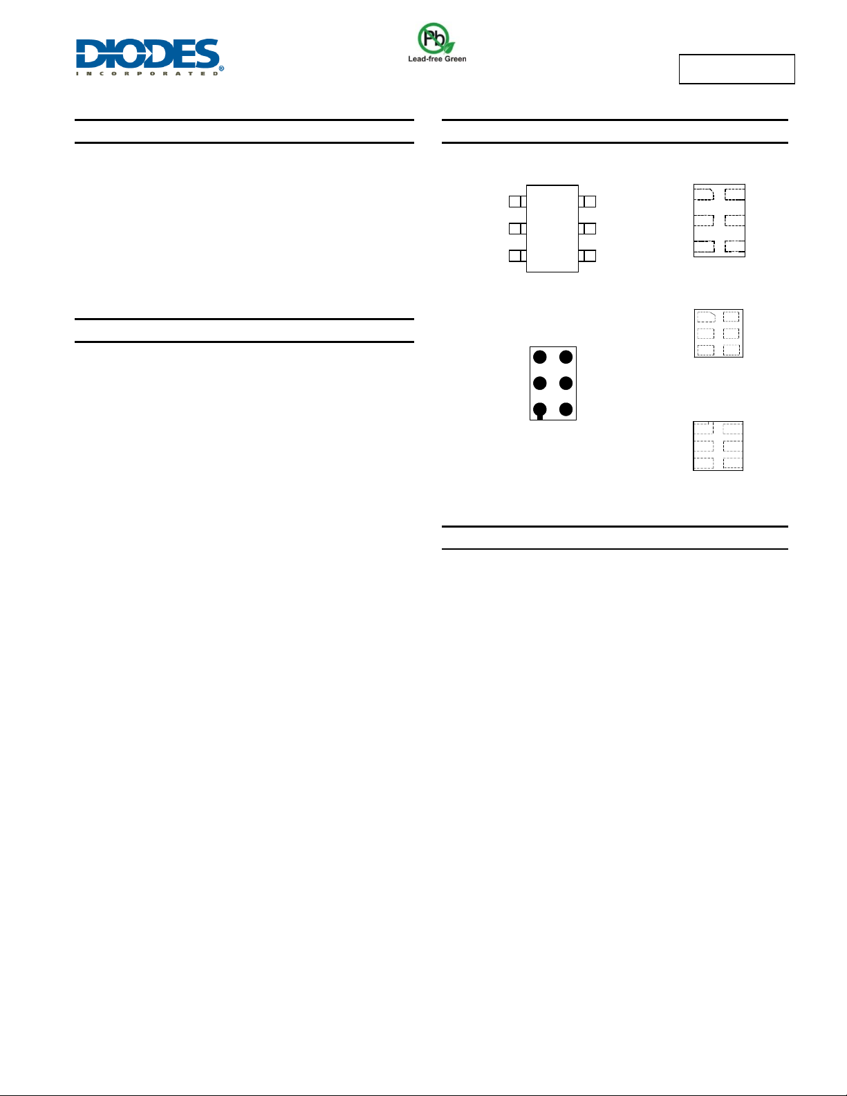
Pin Assignments
2
4
5
6
3
1
(
Top View
)
X2-DFN1410-6
DFN1409
Chip Scale
Alternative
1 6
5
4
3
2
(
Bottom View
)
(
Top View
)
X2-DFN1010-6
1
2
3 4
5
6
SOT26 / 363
( Top View )
43
2
1
6
5
GND
2A
1A
GND
2A
1A
Vcc
1Y
2Y
Vcc
1Y
2Y
GND
2A
1A
Vcc
1Y
2Y
GND
2A
1A
Vcc
1Y
2Y
(Top View)
X1-DFN1010-6
1A
GND Vcc
2Y
1
2
3
4
5
6
2A
1Y
Applications
Voltage Level Shifting
General Purpose Logic
Power Down Signal Isolation
Wide array of products such as:
PCs, Networking, Notebooks, Netbooks, Tablets
Computer Peripherals, Hard Drives, SSD, CD/DVD ROM
TV, DVD, DVR, Set-Top Box
Cell Phones, Personal Navigation / GPS
MP3 Players, Cameras, Video Recorders
Notes: 1. No purposely added lead. Fully EU Directive 2002/95/EC (RoHS) & 2011/65/EU (RoHS 2) compliant.
2. See http://www.diodes.com/quality/lead_free.html for more information about Diodes Incorporated’s definitions of Halogen- and Antimony-free, "Green"
and Lead-free.
3. Halogen- and Antimony-free "Green” products are defined as those which contain <900ppm bromine, <900ppm chlorine (<1500ppm total Br + Cl) and
<1000ppm antimony compounds.
页面指南