
下载
Application Report
SLAA618–November 2013
Implementation of FSK Modulation and Demodulation
using CD74HC4046A
Mahendra Patel............................................................................................. Standard Linear and Logic
ABSTRACT
In telecommunications and signal processing, frequency modulation (FM) is encoding of information on a
carrier wave by varying the instantaneous frequency of the wave. Digital data can be encoded and
transmitted via carrier wave by shifting the carrier's frequency among a predefined set of frequencies—a
technique known as frequency-shift keying (FSK). FSK is widely used in modems, radio-teletype and fax
modems, and can also be used to send Morse code.
Frequency-shift keying (FSK) is a frequency modulation scheme in which digital information is
transmitted through discrete frequency changes of a carrier wave. This application report discusses logic-
level implementation of binary FSK (BFSK) modulator and demodulator using a phase-locked loop PLL
device – CD54HC4046A, CD54HCT4046A, CD74HC4046A, and CD74HCT4046A (hereafter in this
document referred to as HC/HCT4046A). BFSK is the simplest FSK, using a pair of discrete frequencies
to transmit binary information.
spacer
Contents
1 Introduction .................................................................................................................. 2
2 Implementation of Modulator .............................................................................................. 3
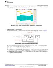
3 Implementation of Demodulator ........................................................................................... 5
4 Test Circuit Waveforms .................................................................................................... 6
5 Schemes To Realize Modulator – Demodulator Pair ................................................................. 10
6 Conclusion .................................................................................................................. 12
List of Figures
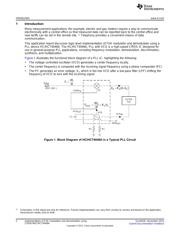
1 Block Diagram of HC/HCT4046A in a Typical PLL Circuit ............................................................ 2
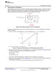
2 Basic Block Diagram of a PLL as a Modulator.......................................................................... 3
3 Frequency Characteristics of VCO Operating without Offset ......................................................... 3
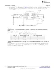
4 Typical Modulator Schematic.............................................................................................. 4
5 Basic Block Diagram of PLL as Demodulator........................................................................... 5
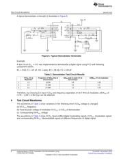
6 Typical Demodulator Schematic .......................................................................................... 6
7 Scheme 1................................................................................................................... 10
8 Scheme 2................................................................................................................... 11
9 Level-Shifter Circuit using LP211 ....................................................................................... 11
10 Simulated Waveforms of Level-Shifter Circuit using LP211 ......................................................... 11
List of Tables
1 Modulator Test Circuit Results ............................................................................................ 4
2 Demodulator Test Circuit Results......................................................................................... 6
3 Variation in VCO
OUT
Frequency, Peak-to-Peak Voltage and DEM
OUT
................................................ 7
4 VCO
IN
(Modulating), VCO
OUT
(Modulated) and DEM
OUT
(Demodulated).............................................. 8
1
SLAA618–November 2013 Implementation of FSK modulation and demodulation using
CD54/74HC/HCT4046A
Submit Documentation Feedback
Copyright © 2013, Texas Instruments Incorporated