

下载
Semiconductor Components Industries, LLC, 2002
April, 2002 – Rev. 0
1 Publication Order Number:
AND8085/D
AND8085/D
An Introduction to FST
Prepared by
Fred Zlotnick
ON Semiconductor
Fast Switch Technology (FST) was introduced into the
marketplace in the early nineties and has become quite
popular with the networking and computing design
community to solve many specialized problems. Will Booth
of Insight Onsite claims the market was nearly $200 M in
the year 2000, and expected to continue to grow over the
next ten years. FST is the dominant bus switch technology,
prevailing over the less popular CBT (Cross Bar
Technology). FST is manufactured by ON Semiconductor
and several other important suppliers.
FST is very simply logic reduced to switches. Several
3–state devices and buffers/multiplexers are constructed
using N–Channel switches instead of logic. The result is the
same logic function, with nearly zero delay. Although, this
sounds perfect, the FST device has no drive capabilities of
its own, but merely passes a signal along, more or less
unimpeded.
2.2 V
2.2 V
00
+5 V
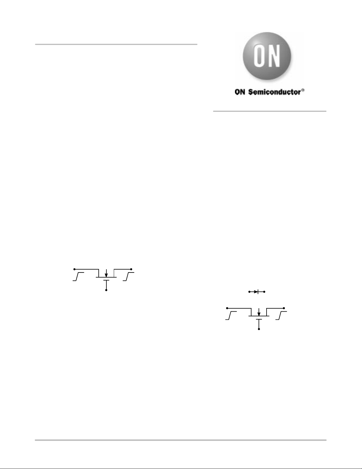
Figure 1.
For those of you who want to understand the why and how
of this family, this diagram shows a single N–Channel FET
switch, biased at +5.0 V at the gate. A signal will pass
through the device, or not, depending upon the bias of the
gate. Interestingly, the FET can conduct in either direction
and unlike a logic gate the time it takes for a signal to pass
through this gate is close to zero. Another interesting
property is this FET, which acts just like a 5.0 V
switch, until
the voltage reaches close to the supply voltage (Vcc). If the
voltage on the left were to reach 4.3 volts, the output will be
limited to within one Vφ of supply or approximately
4.3 volts. This would at first seem to be a stumbling block,
however, remember that many 5.0 volt circuits are “TTL”
compatible and any voltage > 2.2 volts is redundant. For
“CMOS” compatible circuits, the input must exceed
3.5 volts, so 4.3 V is not much of a problem. In fact, this
phenomenon, called ‘body effect’ can be used to your
advantage. If the FST has a Vcc–Vφ as its supply, by
inserting a diode in series with its supply, then, the drop will
be
1.5 V. If one side of the FET were connected to a TTL
compatible, 5.0 V device and the other were connected to a
standard CMOS device operating at 3.3 V, then the FST
device would limit the voltage seen by the CMOS device,
but the 3.3 V output would flow unimpeded to the TTL
device. This then becomes a nearly perfect logic level
translator, with almost zero delay (when turned on).
+3.5 V
+5 V
00
+5 V
Figure 2.
+5 V +V
CC
APPLICATION NOTE
http://onsemi.com