
下载

© Semiconductor Components Industries, LLC, 2013
September, 2013 − Rev. 7
1 Publication Order Number:
2N3055A/D
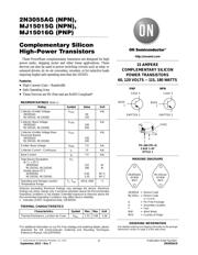
2N3055AG (NPN),
MJ15015G (NPN),
MJ15016G (PNP)
Complementary Silicon
High-Power Transistors
These PowerBase complementary transistors are designed for high
power audio, stepping motor and other linear applications. These
devices can also be used in power switching circuits such as relay or
solenoid drivers, dc−to−dc converters, inverters, or for inductive loads
requiring higher safe operating area than the 2N3055.
Features
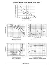
• High Current−Gain − Bandwidth
• Safe Operating Area
• These Devices are Pb−Free and are RoHS Compliant*
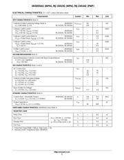
MAXIMUM RATINGS (Note 1)
Rating
Symbol Value Unit
Collector−Emitter Voltage
2N3055AG
MJ15015G, MJ15016G
V
CEO
60
120
Vdc
Collector−Base Voltage
2N3055AG
MJ15015G, MJ15016G
V
CBO
100
200
Vdc
Collector−Emitter Voltage Base
Reversed Biased
2N3055AG
MJ15015G, MJ15016G
V
CEV
100
200
Vdc
Emitter−Base Voltage V
EBO
7.0 Vdc
Collector Current − Continuous I
C
15 Adc
Base Current I
B
7.0 Adc
Total Device Dissipation
@ T
C
= 25_C
2N3055AG
MJ15015G, MJ15016G
Derate above 25_C
2N3055AG
MJ15015G, MJ15016G
P
D
115
180
0.65
1.03
W
W
W/_C
W/_C
Operating and Storage Junction
Temperature Range
T
J
, T
stg
−65 to +200
_C
Stresses exceeding Maximum Ratings may damage the device. Maximum
Ratings are stress ratings only. Functional operation above the Recommended
Operating Conditions is not implied. Extended exposure to stresses above the
Recommended Operating Conditions may affect device reliability.
1. Indicates JEDEC Registered Data. (2N3055A)
THERMAL CHARACTERISTICS
Characteristics Symbol Max Max Unit
Thermal Resistance, Junction−to−Case
R
q
JC
1.52 0.98
_C/W
*For additional information on our Pb−Free strategy and soldering details, please
download the ON Semiconductor Soldering and Mounting Techniques
Reference Manual, SOLDERRM/D.
15 AMPERE
COMPLEMENTARY SILICON
POWER TRANSISTORS
60, 120 VOLTS − 115, 180 WATTS
http://onsemi.com
MARKING DIAGRAMS
2N3055AG
AYWW
MEX
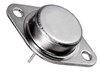
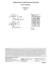
TO−204 (TO−3)
CASE 1−07
STYLE 1
2N3055A = Device Code
MJ1501x = Device Code
x = 5 or 6
G = Pb−Free Package
A = Assembly Location
Y = Year
WW = Work Week
MEX = Country of Origin
MJ1501xG
AYWW
MEX
See detailed ordering and shipping information in the package
dimensions section on page 5 of this data sheet.
ORDERING INFORMATION
PNP
BASE
1
EMITTER 2
CASE 3
BASE
1
EMITTER 2
CASE 3
2
CASE
1
NPN