
下载

Semiconductor Components Industries, LLC, 2003
February, 2003 - Rev. 2
1 Publication Order Number:
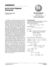
AND8099/D
AND8099/D
5.0 V, 2.0 A Flyback
Converter
Prepared by: Kristie Valdez
ON Semiconductor
The design of a switching power supply is an iterative
process which involves many variables that have to be
adjusted in order to obtain an optimized solution. However,
there are trade-offs which allow for a simple low cost, low
component, single sided board design method. This
application note provides a simple approach to designing
a converter utilizing the ON Semiconductor NCP1055
high voltage switch regulator. The easy-to-follow
step-by-step procedure guides the user into designing the
different blocks that constitute the power supply, mainly the
input block, the power stage, the magnetics, the snubber, the
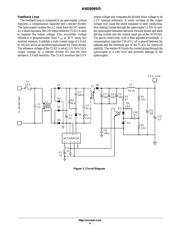
output block, and the feedback loop. The circuit diagram,
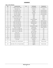
bill of material, and PCB layout are also included at the end
of the application note. This power supply is specifically
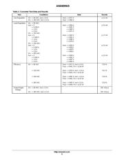
designed for a 5.0 V, 2.0 A output and a maximum duty cycle
of 48%. It meets IEC and UL requirements. EMI is minimal
and a 70% achievable efficiency or greater is possible.
The NCP1055 is a family of monolithic high voltage
switching regulators designed to work in rectified AC line
sources and flyback converter applications. They are
capable of providing an output power ranging from 6.0 W to
40 W with a fixed AC input of 100 V, 115 V, or 230 V
and 3.0 W to 20 W with a variable AC input ranging from
85 V to 265 V. This device features an on-chip 700 V
SENSEFET power switch circuit, an active startup
regulator circuit which eliminates the need for an auxiliary
bias winding on the converter transformer, fault logic with
a programmable timer for converter overload protection.
Protective features provide power switch current limiting,
input under voltage lockout with hysteresis, thermal
shutdown, and restart fault detection. For more information,
please contact an ON Semiconductor sales representative or
log on to www.onsemi.com.
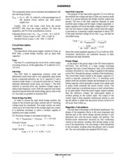
Design Parameters
The first step in designing a power supply is to define and
predetermine the input and output parameters.
Universal Input Voltage Range:
V
in(min)
85 VAC, V
in(max)
265 VAC
Output Specifications:
V
out
5.0 V 2%, I
out
2A
Input Power:
P
in
P
out
est.eff
, an efficiency of 0.78 is a good starting
point for a flyback converter using
MOSFET technology:
P
out
5·2.0 10 W
P
in
10
0.78
12.82 W
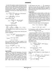
DC Rail Voltages at Low Line and High Line:
V
peak(min)
V
in(min)
·2
85 · 2
120.21 VDC
V
peak(max)
V
in(max)
·2
265 · 2
374.77 VDC
Average Input Current at Low Line:
I
in(avg)
P
in
V
in(low)
,
where V
in(low)
V
peak(min)
V
ripple
V
diode;
I
in(avg)
12.82
80.2
0.160 A
V
ripple
32% V
peak(min)
Input Peak Current:
I
peak
2·I
in(avg)
·
t
sw
t
on
I
peak
2 · 0.160 ·
10 s
4.8 s
0.667 A
APPLICATION NOTE
http://onsemi.com